John Corlett, of the Center for Beam Physics (Group Leader, Beam Electrodynamics Group) is currently working on decreasing size and costs of RF accelerating cavities for the NLC. The state-of-the-art in RF accelerating gradients is currently being achieved with 10 GHz cavities at around 70MV/m. SLAC is working on small RF accelerating structures, known as mm-wave cavites. John’s group has considerable expertise in the design, mathematical charaterization, and fabrication and measurement of RF devices. He’s interested in developing measurement capability in the 90 GHz and higher frequency range.
Wim Leemans, of the Center for Beam Physics (Group Leader, Experimental Beam Physics), is currently conducting research into utilizing pulsed lasers, rather than RF power, to accelerate electron beams. Laser Wakefield acceleration in plasmas offers the potential of developing ultra-compact accelerators capable of producing high quality relativistic electron beams. Acceleration of electrons to energies as high as 100 MeV over mm-size distances has been demonstrated in several experiments. These energy gains correspond to accelerating electric fields in plasmas greater than 30 GV/m.
The accelerating technique that Wim’s group is developing utilizes a plasma channel to guide the electrons accelerated in the wake field of the pulsed laser. The plasma channel is created by striking a gas plume with pulsed lasers that ionize and heat the gas to create a plasma with a cylindrical density distribution. In current experiments, the gas plume is created by puffing gas (hydrogen, helium, or nitrogen) through a nozzle in 100 m-sec long bursts. The conical plume is 1 to 2 mm in diameter. The acceleration of the electrons is limited by the non-uniform density distribution in the gas and the short length of the plume. Wim’s group is currently building a gas jet test stand to test nozzle and valve designs. The current nozzle is conventionally machined with a bore diameter of 750 microns. The gas bursts are created with a poppet-type solenoid valve (1000 psi backing pressure). Wim hopes to test new nozzle designs as well as a piezoelectric valve with a faster opening and closing time (30-40 microseconds).
Wim views the gas jet technology as critical to the continued development of Laser Wakefield acceleration at LBNL. He is particularly interested in the possibility of developing technologies to shape the density distribution of the gas plume and make it longer. Ideally, the gas plume would have a length of several centimeters and a width of 100 to 200 microns. If longer plumes can be produced, it would also be useful to adjust the density of the gas along the length of the plume. The electrons gain velocity as they are accelerated in the plasma channel. The speed of propagation of the laser in the gas medium decreases with gas density. If the gas density is uniform throughout the length of the plume, the accelerated electrons will outpace the laser. If the gas plume were created by a linear array of independently controlled nozzles, the density profile could be adjusted to balance the plasma density with the propagation speed of the laser, yielding optimal acceleration of electrons.
The micron scale nozzles and valves currently under development in the MEMS field may be applicable to the gas jet project. In theory MEMS microfluidic devices are of an appropriate physical scale and could have the advantages of fast actuation (by virtue of the low inertia of moving parts) and independent control. Assuming few components or existing designs would be readily available for a MEMS solution to this problem, significant engineering and testing may be required to create a working system.
Biology – Marty
MEMS is a very active area in the life sciences. There are currently several companies engaged in producing commercial products. Conferences in the life sciences often have short courses in MEMS areas such as microfluidics, labs on chips, microarrays, etc. The dimensional ranges for MEMS devices is well matched for the life sciences. Large macromolecules define the small end of the dimensional range and individual cells the large end of the range.
There is currently a mature commercial presence in the microarray area. Affymetrix and other companies sell DNA microarrays and microarray services. Automation readily exists for this application. Molecular separation is another area where there is a large commercial effort though there are few products on the market. Applications vary from DNA sequencing to DNA sizing to genotyping.
Biological diagnostics is a very large area with great potential for work opportunities. Diagnostic devices for identifying pathogens are needed for the domestic and military medical community. Diagnostics covers the entire range of sensor types that are applicable in chemical analysis: pH, optical, resistivity, fluorescent detection, etc. These could be devices located in diagnostic labs, doctors offices, or devices carried by individuals or implanted in individuals. Manipulation and experimentation of individual cells is an area of current interest. There could be applications in human and livestock fertilization and diagnostics.
One model for a future LBNL project in this area would be for engineers to team up with a Life Sciences/Genomics principal investigator and also with a commercial company. A company like Caliper Technologies is primarily interested in the chip manufacturing and not in the robotics or general machine design. LBNL could design and build the machine around a chip for a particular application. An example might be a high throughput PCR machine. Caliper could design the chip and the liquid handling to/from the chip. LBNL could design an instrument with the frame, a robot arm to feed 10’s or 100’s of chips, electronics, motion control, data collection, etc. The advantages of such an instrument we be low reagent usage, low power, and automated sample loading. The chips would be small but the overall instrument may be sizable.
There could be opportunities in the development of process techniques for MEMS devices, mechanical and electronic integration, and data communication. These are research areas that benefit all MEMS applications as well as in the life sciences.
LBNL Fabrication
Capabilities
Building 70A Instrument Support Laboratory (ISL)
The
ISL was constructed in 1994 by LBNL to provide cross-divisional support for
semiconductor detector development and fabrication. This new facility, which is operated by the LBNL Engineering
Division consists of an approximately 500 sq. ft. Class 100 and a 4,000 sq. ft.
Class 10,000 clean room. There is also
a machining room in which a number of saws and other equipment is available for
fabrication of parts. The highlights of
some of the processing and test capability of the ISL that is applicable to
this proposal are given below.
Location:
Class 100 Clean Room
|
Item |
Application |
|
Thermco Furnaces |
Dopant diffusion and silicon oxidation |
|
Quintel photomask aligner |
contact mask aligner for photolithography |
|
Kulicke & Soffa Model 4523 Wirebonder |
Making electrical connections from test electronics to microchips |
|
Headway Research Wafer Spinner |
Spin-coating thin films, e.g. photoresist |
|
Chemical Hoods |
Photolithography, etching, general chemical processing |
|
Nikon Measuring Microscope |
Measurement of features on microchips |
Location: Class 10,000 clean room
|
Evaporators |
Au, Al, Li, Cr, Pd depositions |
|
RF Sputterer |
Si, Ge, Au, Pd, Pt, Cr, W depositions |
|
Electronics test benches |
Semiconductor device evaluation |
|
Filmetrics Thin Film Measurement System |
Determines thickness, n and k using a reflectance measurement |
|
Nikon Metaphot Microscope |
Inspection and measurement of features on microelectronic devices |
|
Chemical Hoods |
Cleaning, etching and general chemical processing |
Location: Machine Room
|
Disco DAD-6HT Dicing Saw |
Wafer dicing and scribing, contact segmentation |
|
Sheffield Cavitron Ultrasonic Machine Tool |
Machining grooves and guard rings in Si(Li) detectors, contact segmentation |
|
SCS Paralene Deposition System |
Passivation of semiconductor devices |
|
Micro-Matic Outside Diameter (O.D.) Diamond Saw |
General shaping and machining of parts |
|
Silicon Technology Corporation Inside Diameter (I.D.) Saw |
Slicing of silicon wafers from silicon boules |
Building 77 Main Shop
Roku-Roku (GG-435N) - High Speed NC Machining Center
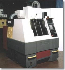
Location Building 77 Tool Maintenance Room, Contact: Norman Salmon
Positioning Accuracy: +/- 2 microns per full stroke
Repeatability: +/-.5 microns
Resolution: 100 microns
Spindle Speed: 36,000 RPM
General Description: Norman Salmon (e-mail 10/10/01)
The machine has resolution to .0001 mm . The repetability is more like .5 micron and accuracy is aroun 1 micron. This is very subject to the type of features milled or drilled. One example is drilling 1000 holes to that are 110 microns diameter to 2 micron pitch accuracy with standard deviation of 1 micron on diameter. Milled features depending on the size are more challenging due to dimensions of the tooling, however with good practice 1-2 microns accuracy are possible. It just depends on the case. I have cut steps across a part with 10 millionths steps. You also have to consider temperature changes and true position which make it more challenging on parts that require long durations.
This machine overall is extremely good as far as milling machines go. If there is a desire to improve on this we can tighten this up on this machine with some modifictions. If there is a need/desire to push beyond this there are some alternative processes in EDM which will push sub micron accuracy and yield features in the 10-20 micron range where as we are limited to 40-50 microns on drills at 100 microns on endmills in metallic materials and 50 microns plastic/graphite.
Keyence Digital HD Microscope (VH-8000)
http://www.keyenceup.com/vh8000/index.html
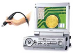
Location: Building 77, Design Works, Contact: Ken Chow
A portable digital microscope with an integral 15-inch high-definition LCD monitor. The lensesre available with magnification ranging from 0x to 3000x (LBNL head ased with microscope has 175X magnification).
Image pick-up element: 1/2-inch, 2.11-million-pixel CCD image sensor
Total pixels: 1688 (H) x 1248 (V)
Effective pixels: 1636 (H) x 1236 (V)
Frame rate: 7.5 frames/sec. or 30 frames/sec. (selectable)
Resolution: 1000 lines min. (H/V)
UCB-BSAC
Prof. Liwei Lin